Schematics ... done
after approximately one month ( with many interruption ) the schematics design of KLST_PANDA is done.
this phase also included the specification of all components in accordance to what JLCPCB offers.
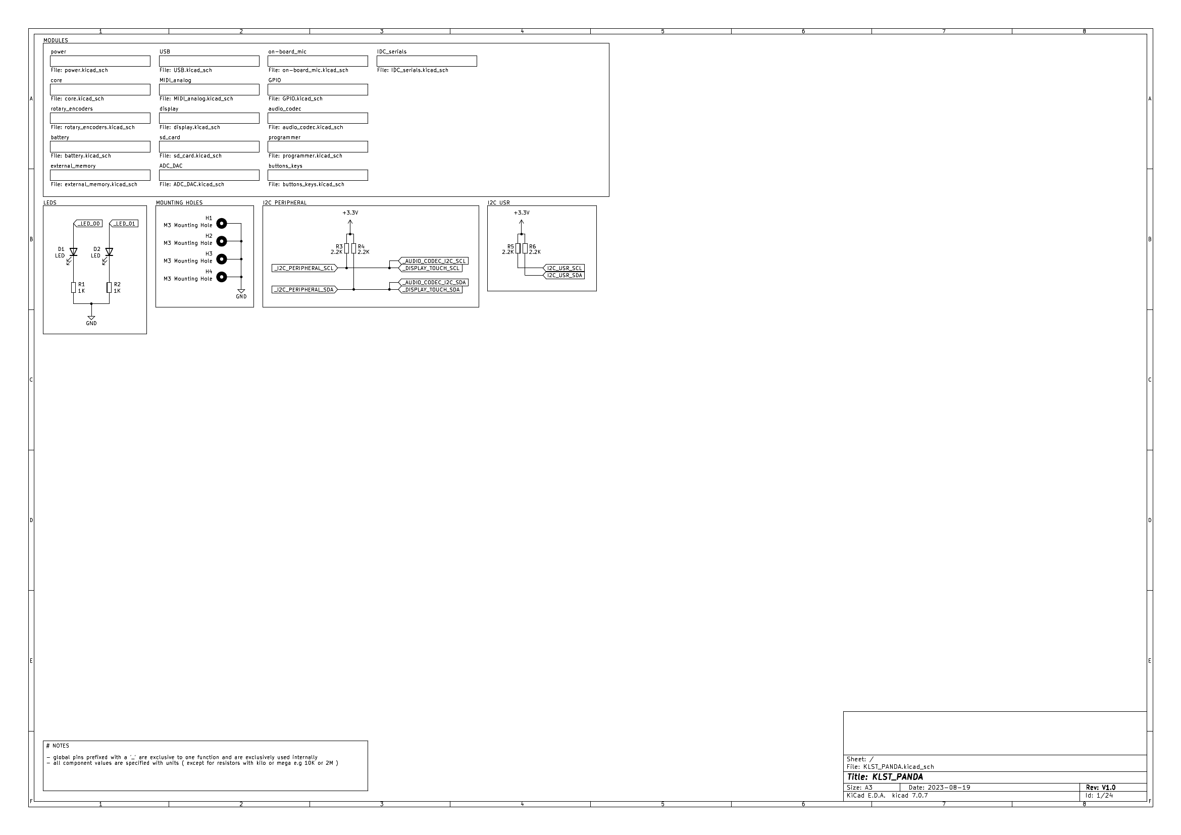
i decided to organize the schematics in pages according to the modules ( e.g core, power, display, audio codec, etcetera ):
Core … done
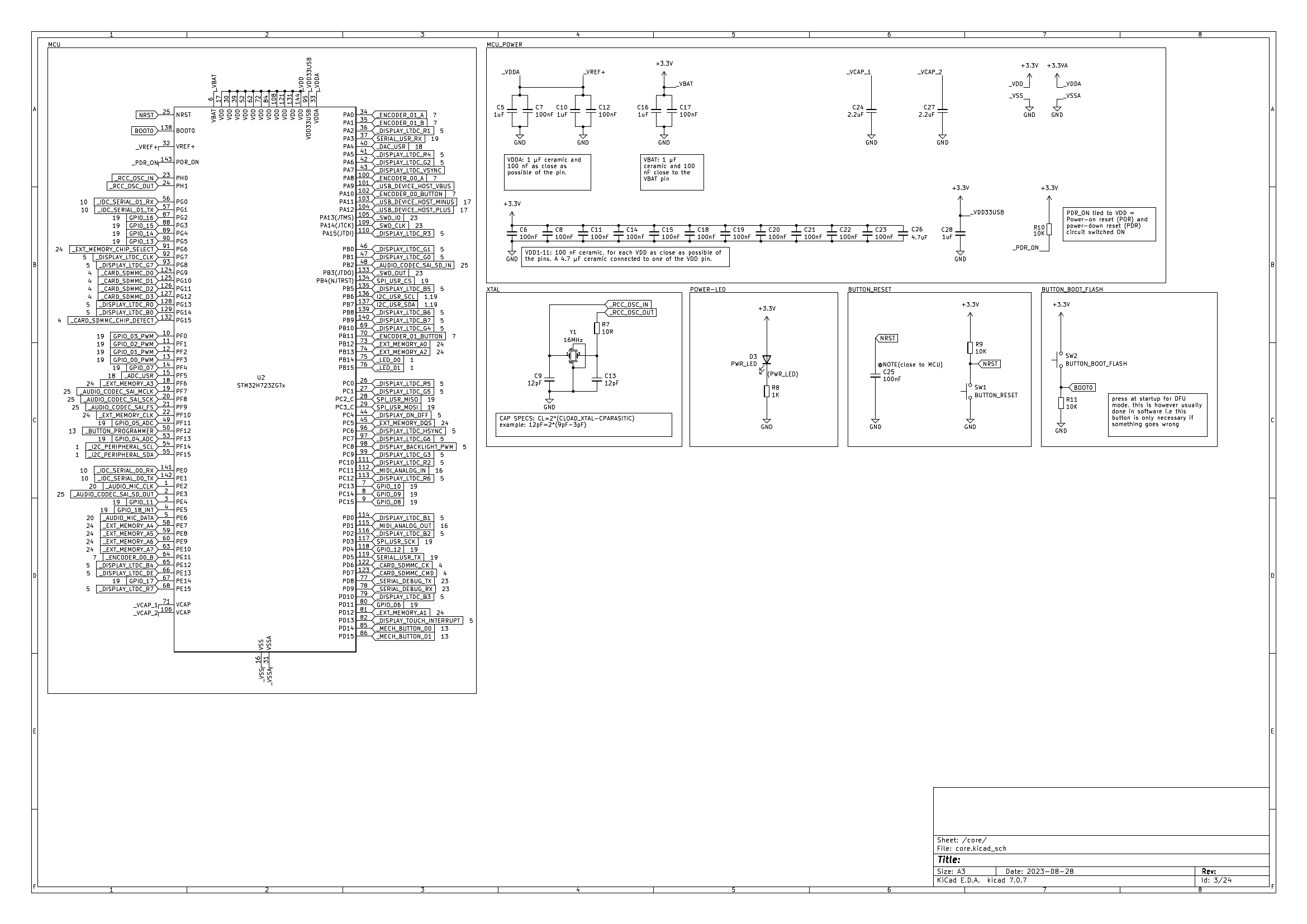
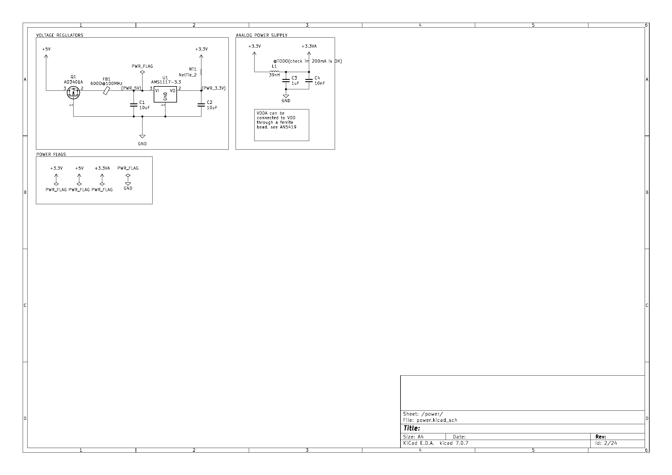
the core is a STM32H723ZGT by ST, a 32-bit Arm® Cortex®-M7 CPU ( or MCU ) with 550MHz, 564KB RAM, 1024KB Flash, and FPU that comes in a LQFP-144 ( 20x20x1.4mm ) package.
what i have learned
well, basically a banality: it is good to read the manual! so i did and found some solid advise on how to connect the core: Getting started with STM32H723/733, STM32H725/735 and STM32H730 Value Line hardware development (AN5419)
furthermore, there is also good help from the schematics of ST’s development boards STM32H735G-DK (MB1520) and # STM32H743I-EVAL (MB1246).
SD Card … done
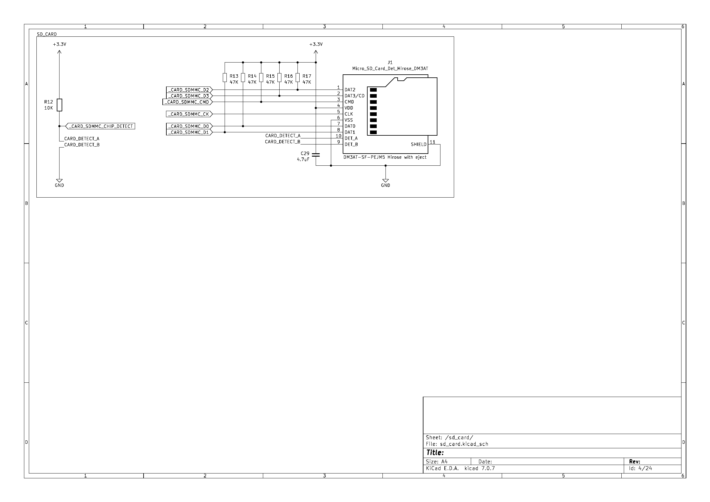
the SD Card supports SDIO/SDMMC with a 4-bit wide data line and an automatic card detect functionality.
Display … done
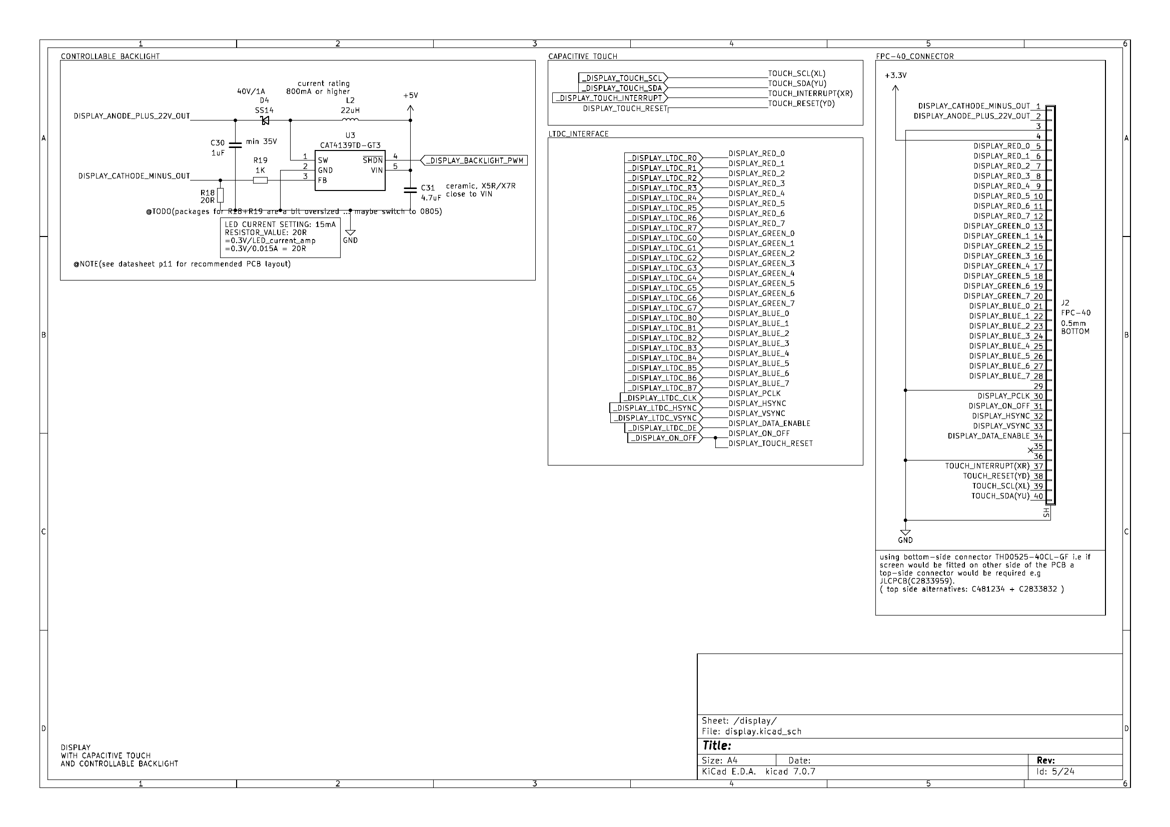
the display is a 4.3” TFT LCD ( ER-TFT043A2-3 ) with a resolution of 480×272px, 24Bit colors. it is connected via a 40-pin FPC connector and features a capacitive touch surface ( interfaced via an FT5206 I2C-based controller ) and dimmable a backlight ( via CAT4139 + PWM ).
the display is interfaced with the CPU via a parallel LTDC interface.
what i have learned
about touch panel interface
it took me some time to realize that despite my earlier assumptions, the capacitive touch panel does not require an external driver, unlike a resistive touch panel, but uses the 4 pins that are otherwise reserved for resistive touch panel interaction ( RESIST. ) for the on-board driver chip FT5206 which communicates via I2C ( SDA + SCL ) with the MCU. the mapping is not documented in the display’s datasheet but it looks like this:
| # | FT5206 | RESIST. | FPC40 |
|---|---|---|---|
| 1 | SDA | YU | 40 |
| 2 | SCL | XL | 39 |
| 3 | RST | YD | 38 |
| 4 | INT | XR | 37 |
| 5 | GND | GND | 36 |
| 6 | VDD | NC | 35 |
i also realized that driver chip is powered by the power pin locate on position 4 on the FPC40 connector
in summary this is quite a nice revelation because most resistive touch panel driver require a chip that connect via SPI. this extra bus i can save now and i am even considering using the same I2C bus that i also allocated for the audio codec thus freeing up some GPIO pins.
about the connector
and a word of warning: i found out that there are 3 types of FPC connectors. those that connect on top, bottom and both sides. this is quite crucial for the design of the PCB. oftentimes the brown flat flexible cable is folded under the display and attached to the PCB together with the display i.e on the same side as the connector. this would then require a bottom-connected FPC connector. occasionally, the cable is threaded through a hole in the PCB or over the PCB’s edge and then connected on the backside of the PCB. such a design would then require a top-connected FPC connector. however, i probably stick with the former.
party knowledge: FPC stands for flexible printed circuit and FFC for flat flex cable both terms are often used interchangeably. the cables are often made from brown polyimide as a product by DuPont also called Kapton.
Battery + Charger … done
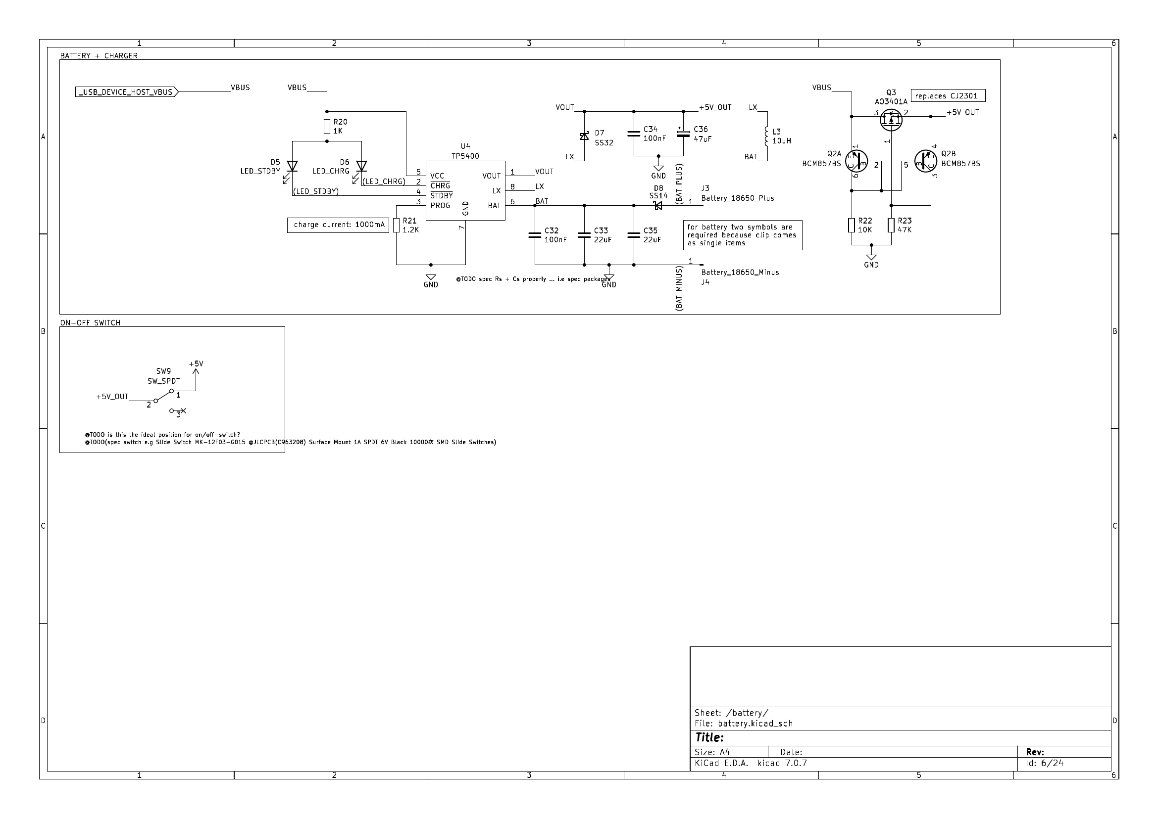
the battery is a type 18650 cell fitted into an on-board battery holder, which allows to easily replace the battery. the battery can be charged via the USB-C connector.
the charging mechanism is realized via a TP5400 an all-in-one battery charger and boost converter IC.
the board also features an on-off switch.
what i have learned
not related to the battery charger alone but i found a nice workflow to convert symbols, footprints and 3D models offered at JLCPCB to KiCad:
- EasyEDA ( export project as KiCad + 3D models )
- WOKWI: Convert EasyEDA Files To KiCad EDA ( convert EasyEDA to KiCad project and 3D files (OBJ) )
- Blender ( convert OBJ files to )
note that blender calls WRML .x3D and is quite a good tool to generate and export 3D models.
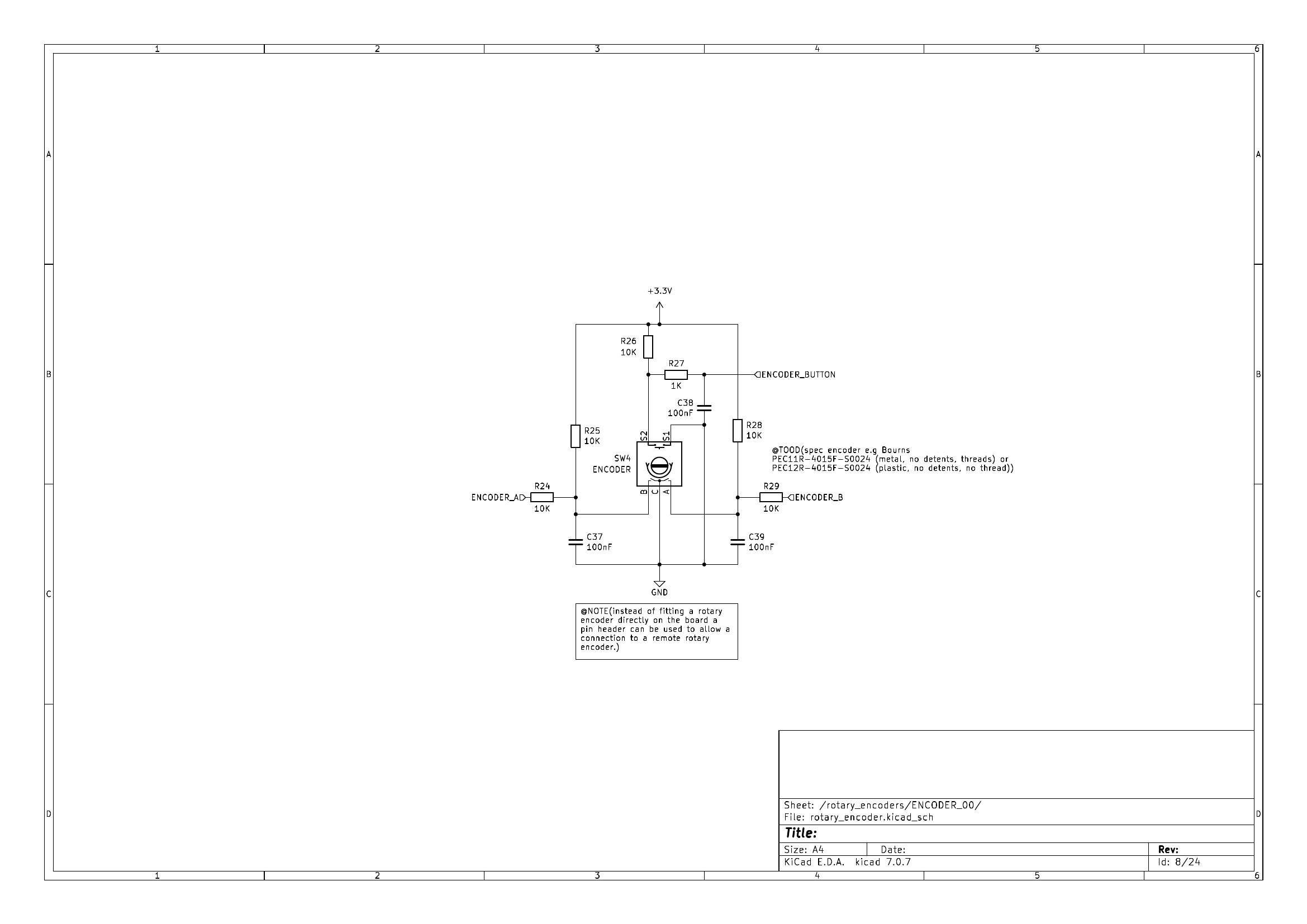
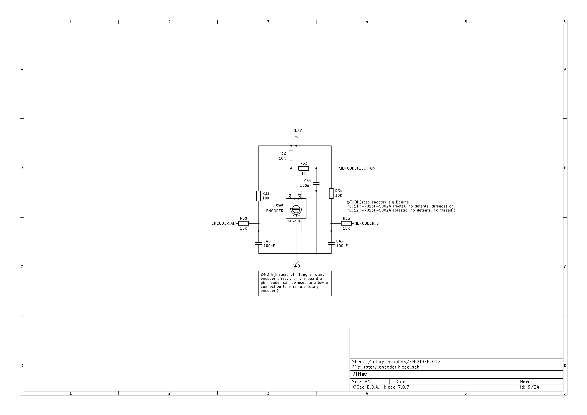
Rotary Encoder … done
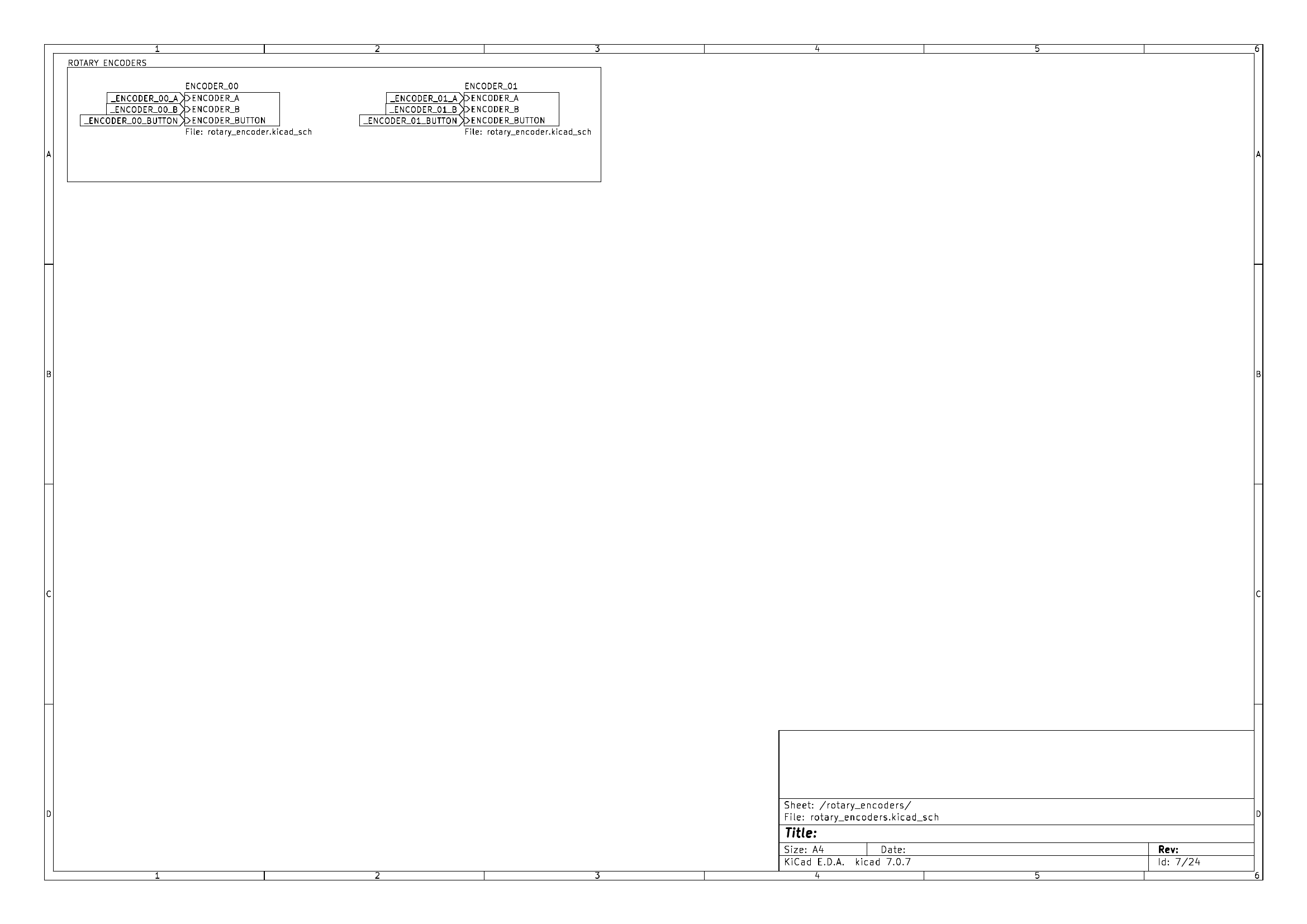
two rotary encoders PEC11R-4015F-S0024 by Bourns feature a 6mm diameter metal shaft, a metal case, a push button and 24 pulses per 360° rotation but no detents.
the encoder body is 6.5mm high, the shaft is 15mm long of which 5mm feature an M7 thread and the top 7mm are D-shaped.
buttons and pulse channels are debounced in hardware.
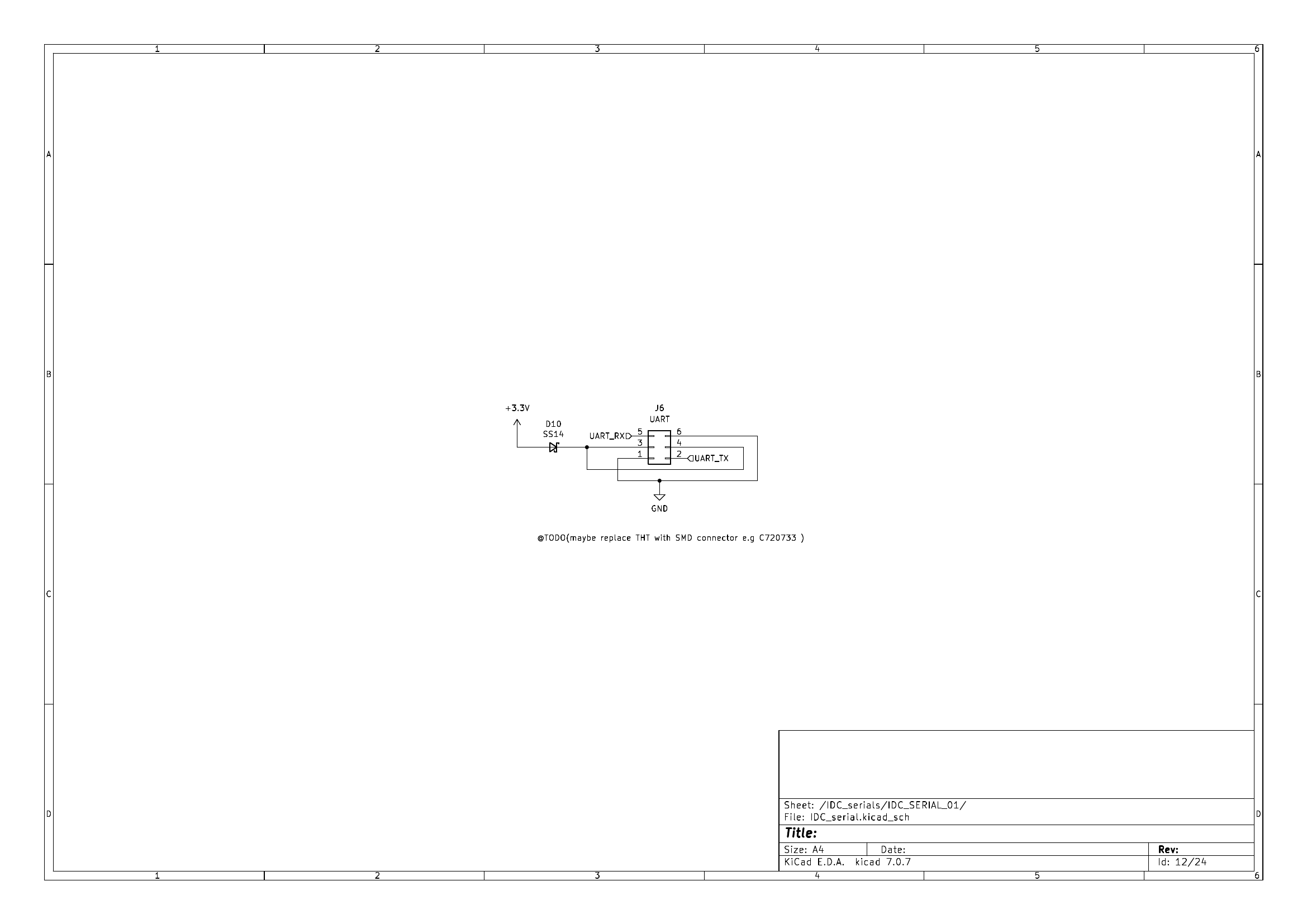
IDC Serials … done
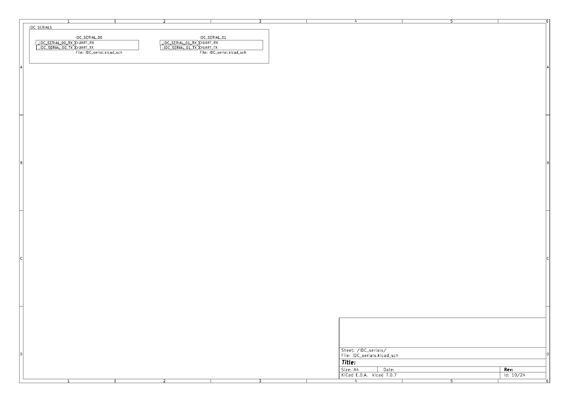
two serial ports are available as 6-pin shrouded IDC connectors. ports can be connected with a crossed cable ( as also used in KLST_SHEEP ).
the pins of the connectors are assigned as follows:
+---------------+
|  GND 1  2 TX  |
|| PWR 3  4 PWR |
|  RX  5  6 GND |
+---------------+

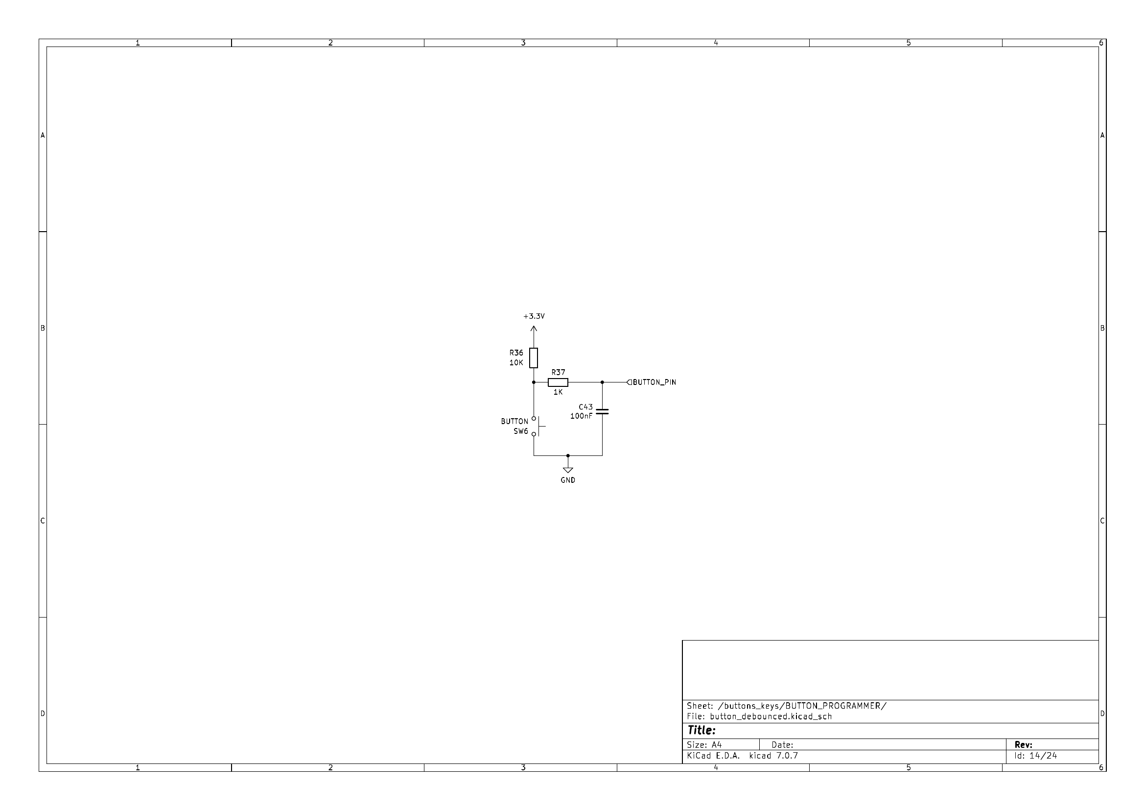
Buttons + Keys … done
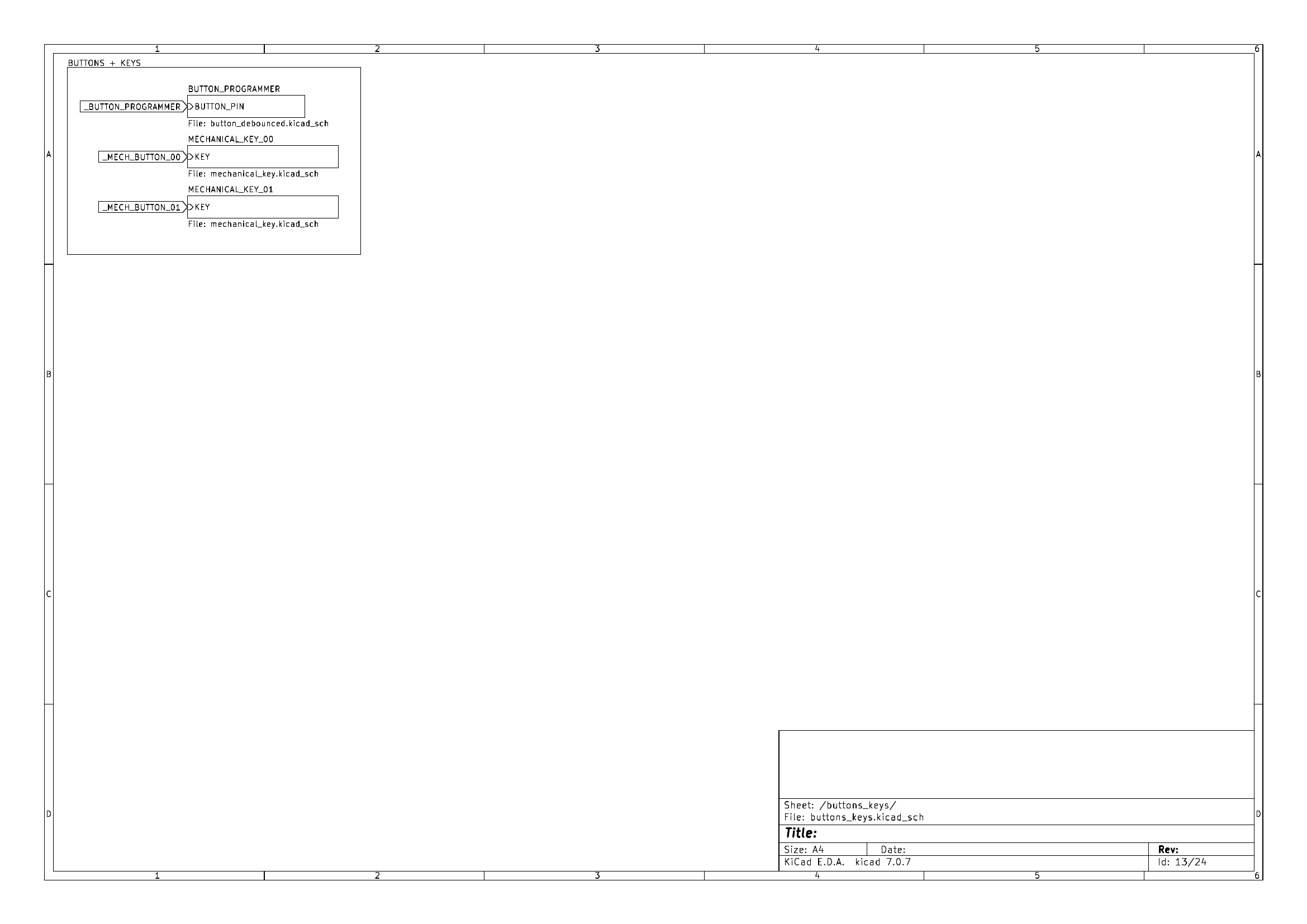
the board is equipped with a RESET button, a BOOT_MODE button and a PROGRAMMER button. if the BOOT_MODE is pressed at start-up the core (MCU) will enter DFU mode. PROGRAMMER button can trigger DFU mode at runtime. the RESET button triggers a soft reset.
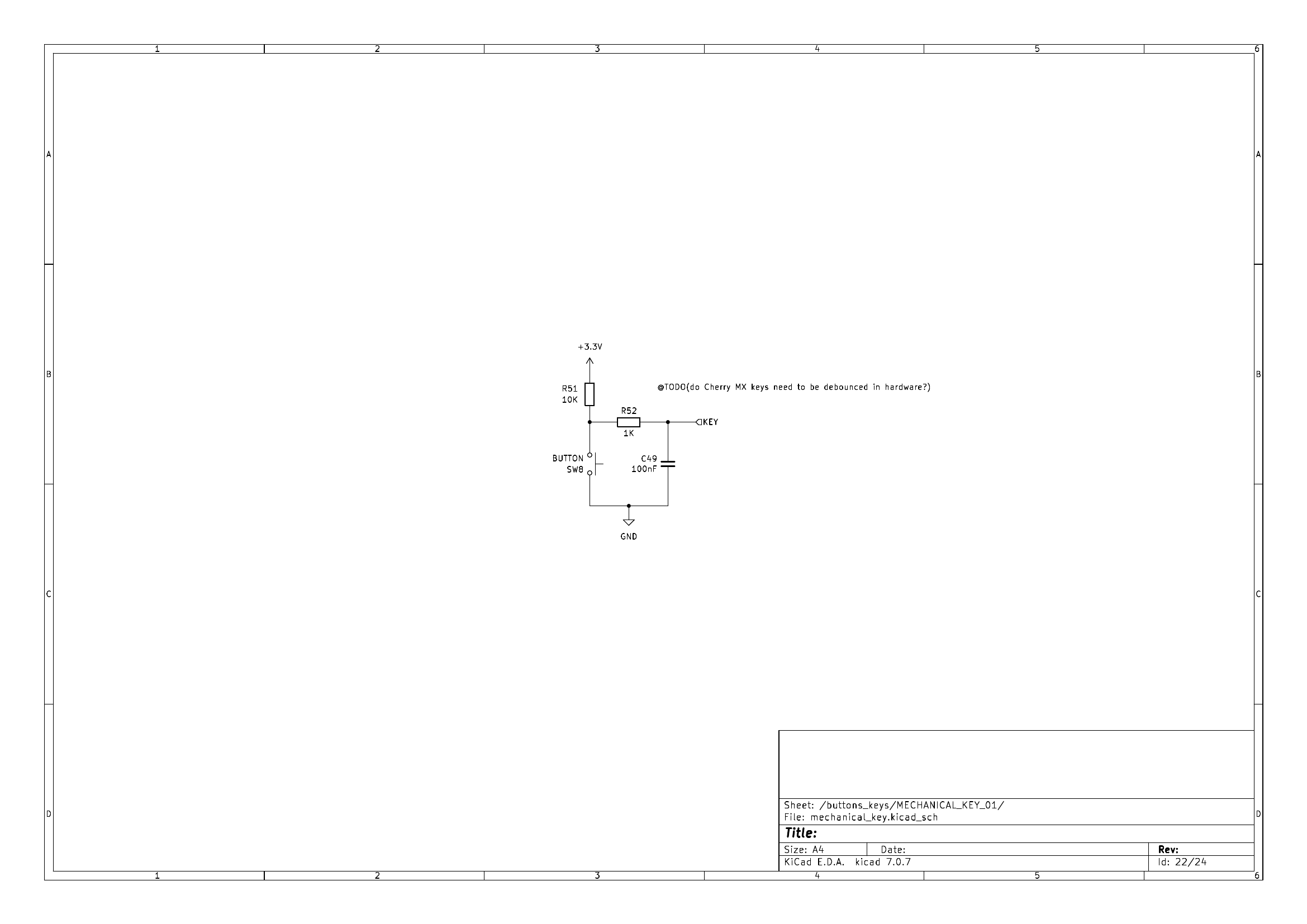
the booard also features two user-programmable mechanical Cherry MX keys. both can be connected to a hardware interrupt.

MIDI ( analog ) … done
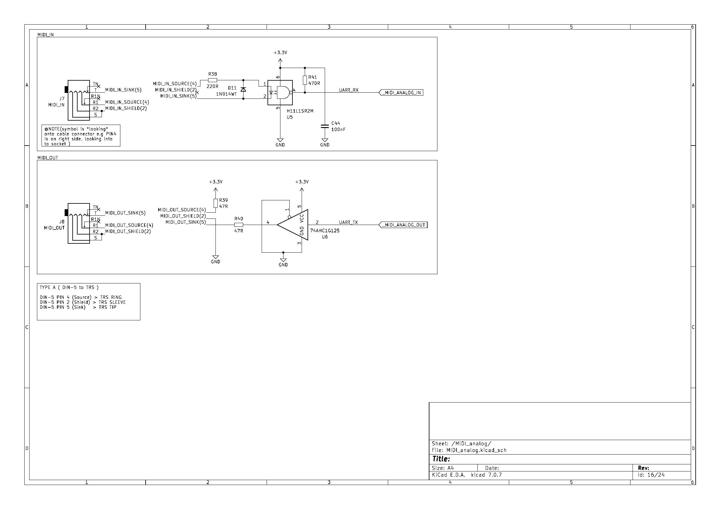
an analog MIDI-IN and a MIDI-OUT connector ( both via UART ) are available through two 3.5mm audio connectors ( TRS with Type A allocation ).
what i have learned
as always … it s complicated. while the MIDI Association apparently defined a mapping for Tip-Ring-Sleeve ( TRS ) audio connectors it is by no means a standard adopted by everyone ( see How TRS MIDI Works ). i am especially annoyed by this as Arturia seems to use a different pin mapping.
USB-C … done
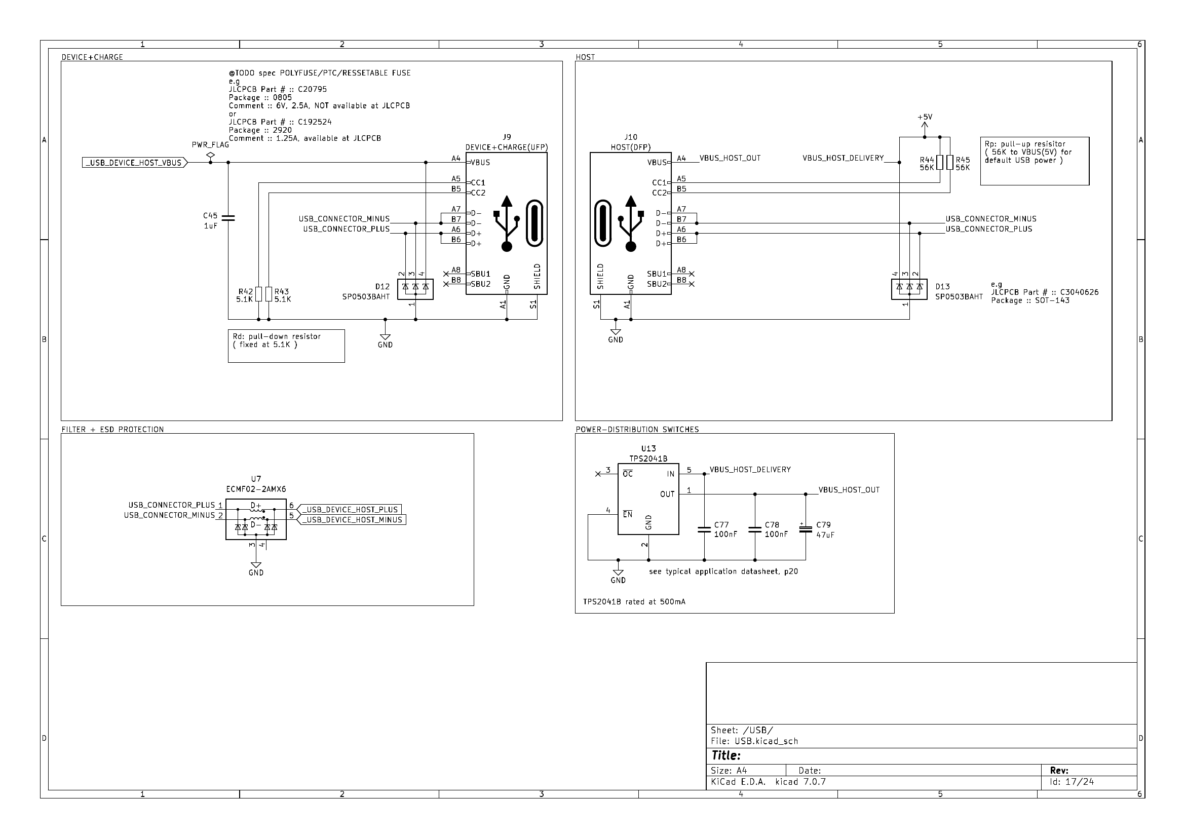
the board features two USB-C connectors. one that acts as USB Device and takes care of the power supply including the charging of the battery, while the other one can be used as a USB Host to connect keyboards, mouse or USB MIDI Devices.
ADC + DAC … done
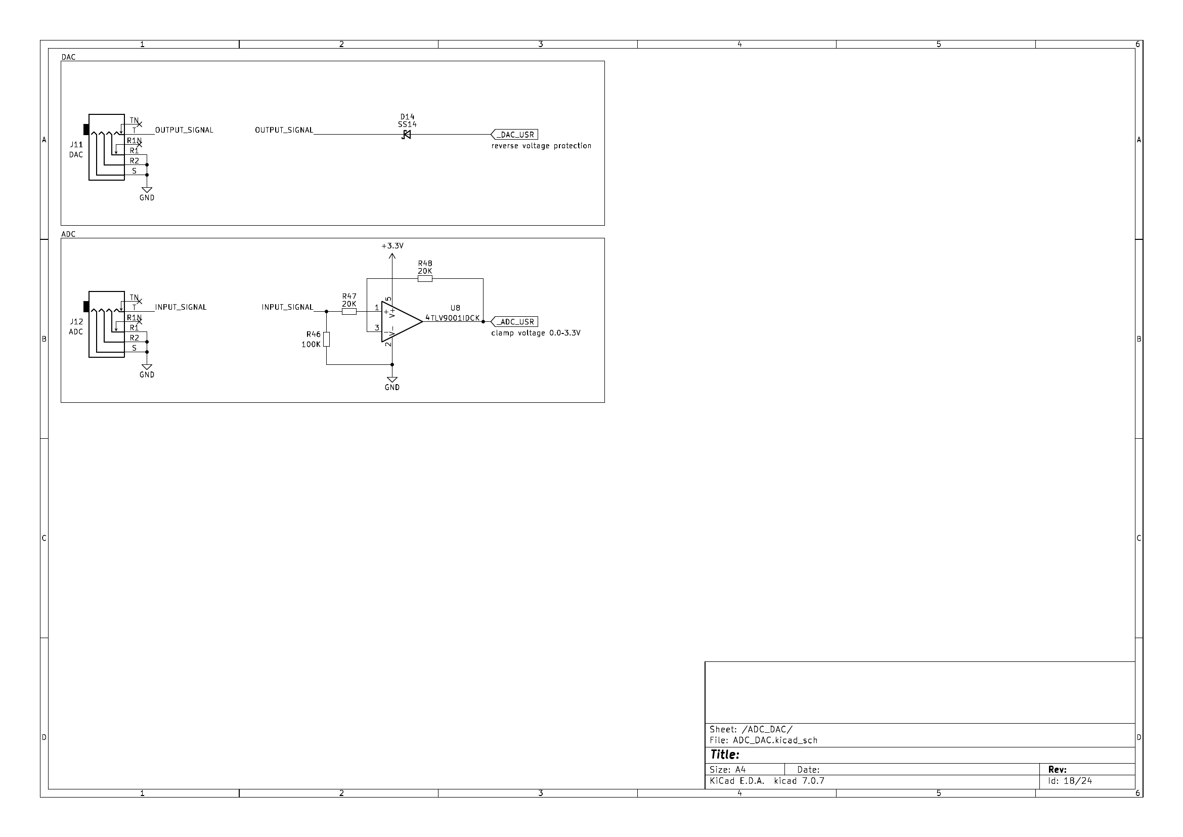
one Digital-Analog-Converter ( DAC ) and one Analog-Digital-Converter ( ADC ) are made available via two 3.5mm audio connectors ( TS ). the DAC can generate voltages from 0.0V–3.3V, while the ADC can measure voltage from 0.0V–3.3V.
what i have learned
electrically speaking it s a bit of a challenge to supply a versatile interface between modular synthesizer world and microcontroller world. it requires quite some effort to achieve the modular voltage range ( -10V–+10V, -5V–+5V ), especially, if not wanting to rely ( for whatever reason ) on the modular power supply. therefore ( and also for compatibility to other contexts ) i decided to keep the 0V–3.3V range of both ADC + DAC. if the ADC + DAC were to interface with a modular synthesizer setup, the attenuation and shifting of the voltage range would need to happen on the modular synthesizer side.
the only measure i took was to protect the DAC against over-voltage by adding an op-amp configured as a buffer.
GPIO … done
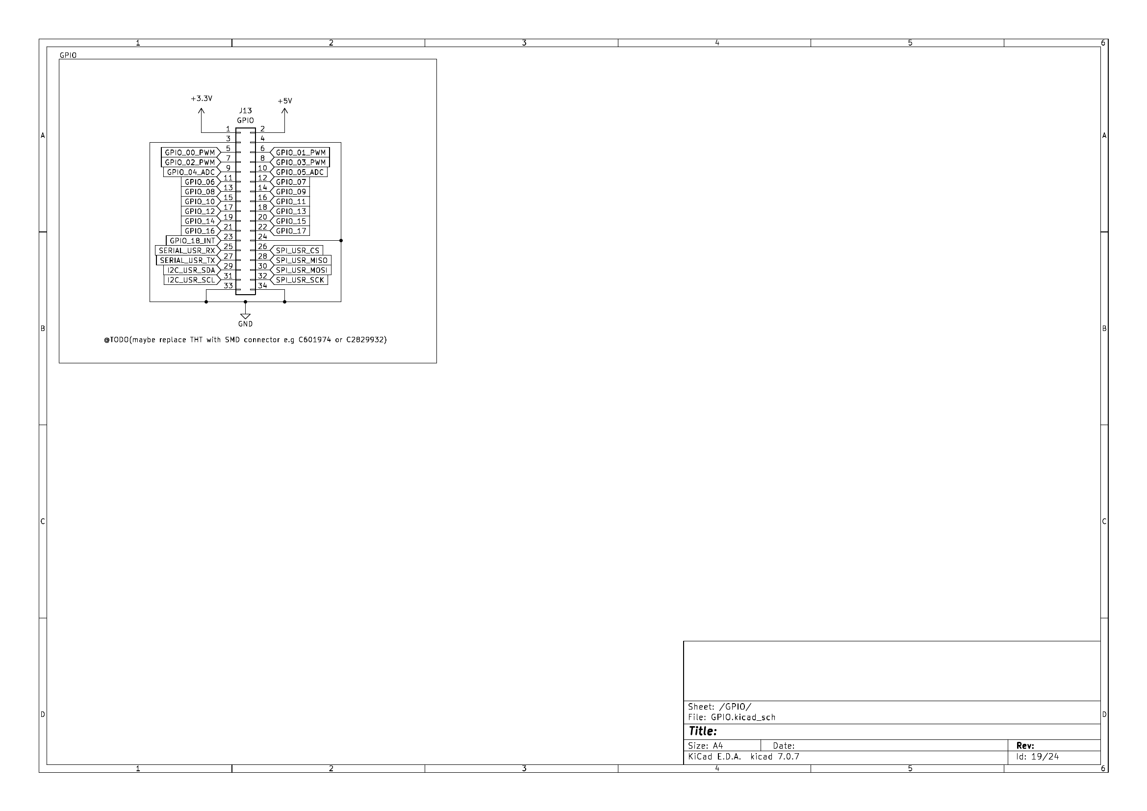
a 34-pin port hosts 28 General Purpose Inputs and Outputs (GPIO) and 6 power pins. the GPIO can either be used as standard input or output pins or can have the following extra functionalities:
- 19× GPIO pins including
- 4× programmable PWM pins
- 2× ADC pins
- 1× external interrupt pin
- 1× USART ( 2 pins )
- 1× SPI ( 4 pins )
- 1× I2C ( 2 pins )
the power pins are available as follows:
- 4× GND
- 1× 3.3V
- 1× 5.0V
the GPIO connector is a shrouded IDC connector.
On-Board Microphones … done
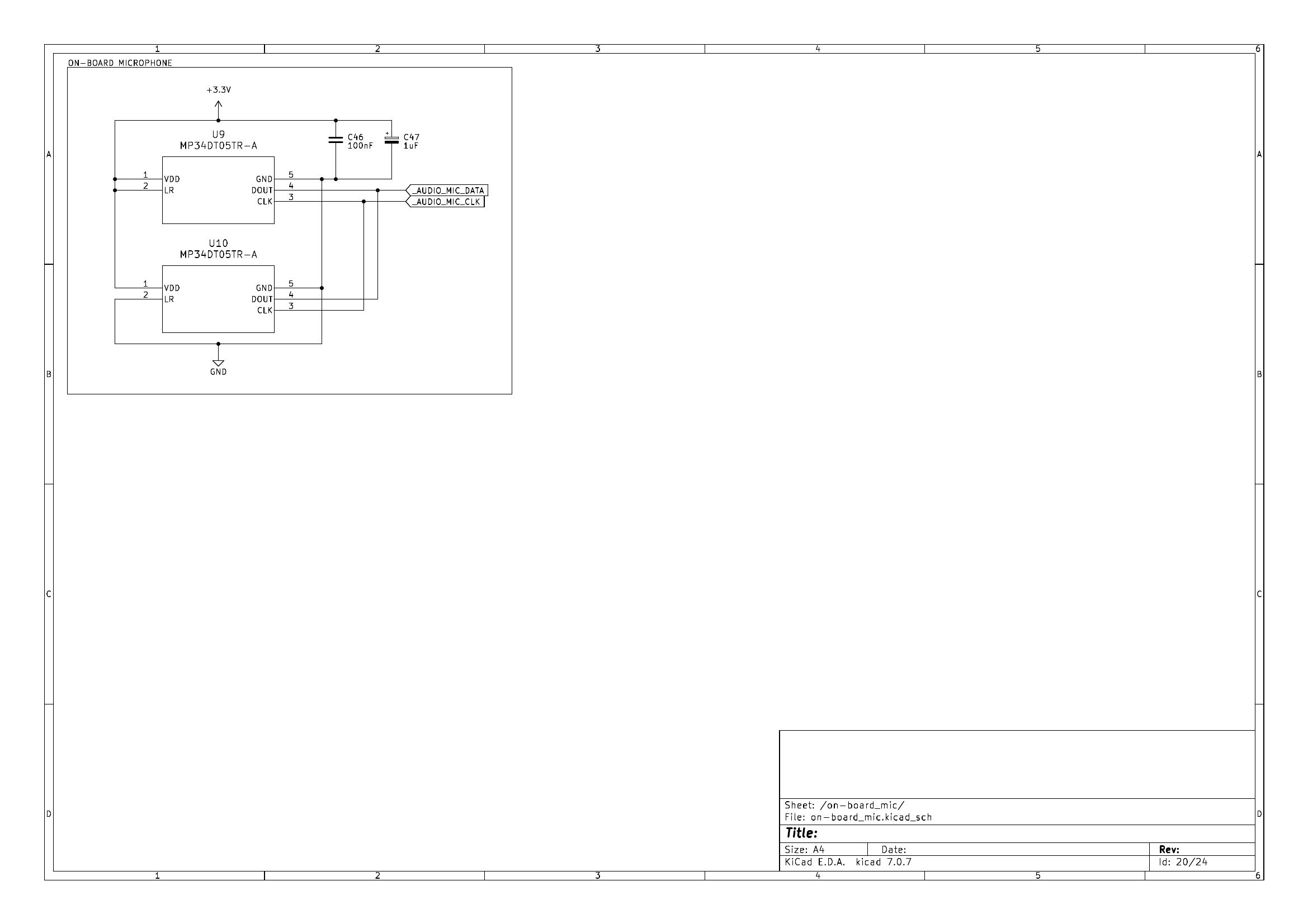
the on-board microphones are two mono MEMS microphone ( MP34DT05TR-A ) fitted directly onto the board and interfaced via a PDM interface. they can be used in parallel with an external microphone or line-in signals from the audio codec.
what i have learned
PDM ≠ I2S/SAI. i had reserved one I2S/SAI bus for the microphones. as it turns out, however, the microphones i was looking at are PDM type microphones which is NOT per se compatible with I2S or SAI. luckily STM32 provides an interface to PDM/PCM devices via SAI, however, requiring less but different pins. after rearranging some pins i ended up freeing 2 pins. nice! furthermore it comes at almost no extra resources to add two instead of one microphone … so i did that two.
Programmer … done
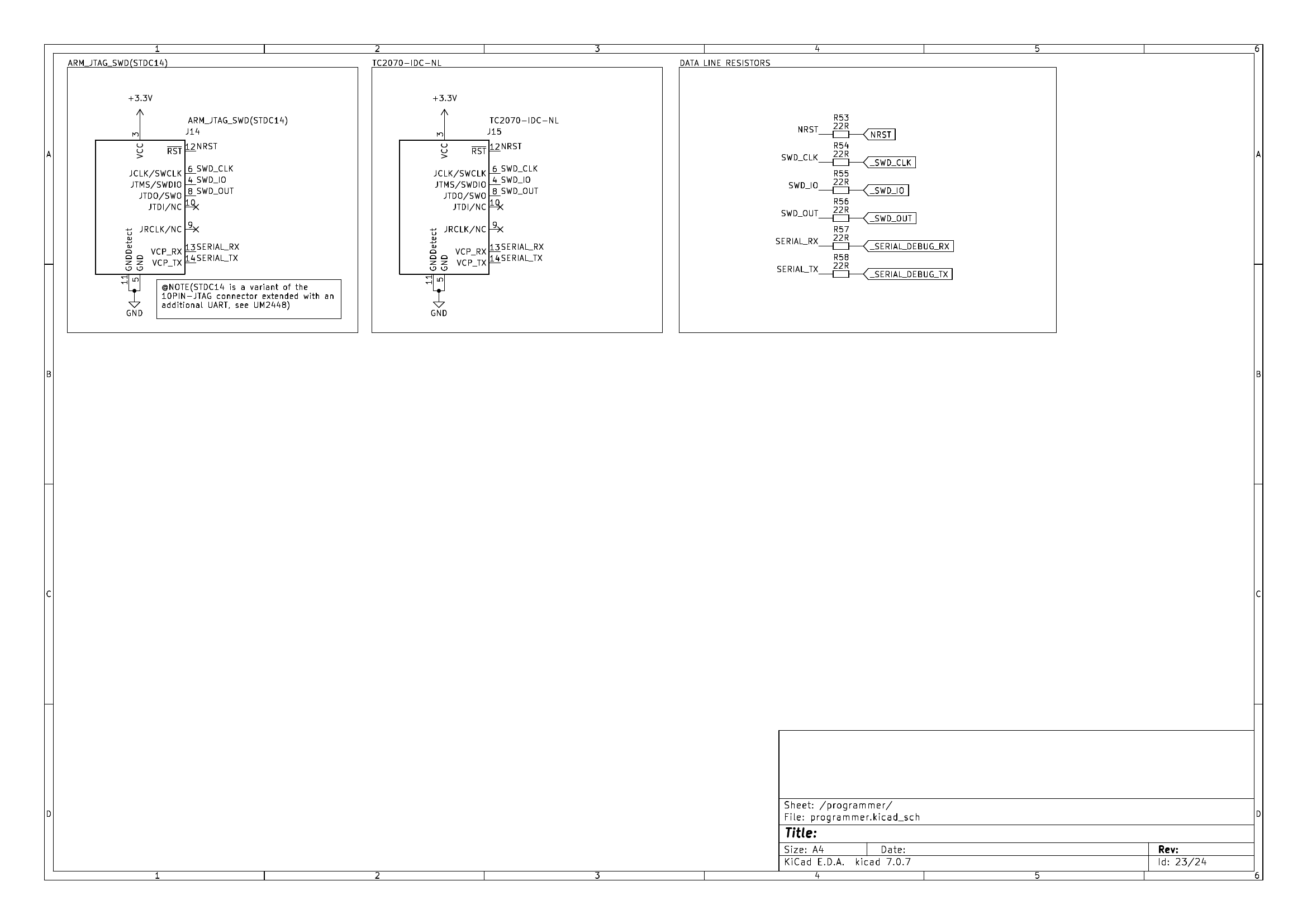
the programmer interface features two options. on one side of the board there is a standard STD14 connector ( a SWD/TAG connector extended by a dedicated serial port for debugging ), while on the other side there is a PCB-only ( no extra hardware components required ) footprint to be used with a TC2070-IDC-NL-050 by Tag-Connect.
what i have learned
not such a big thing but something to be aware of: the STD14 connector and the TC2070-IDC footprint have different pin arrangements.
External Memory … done
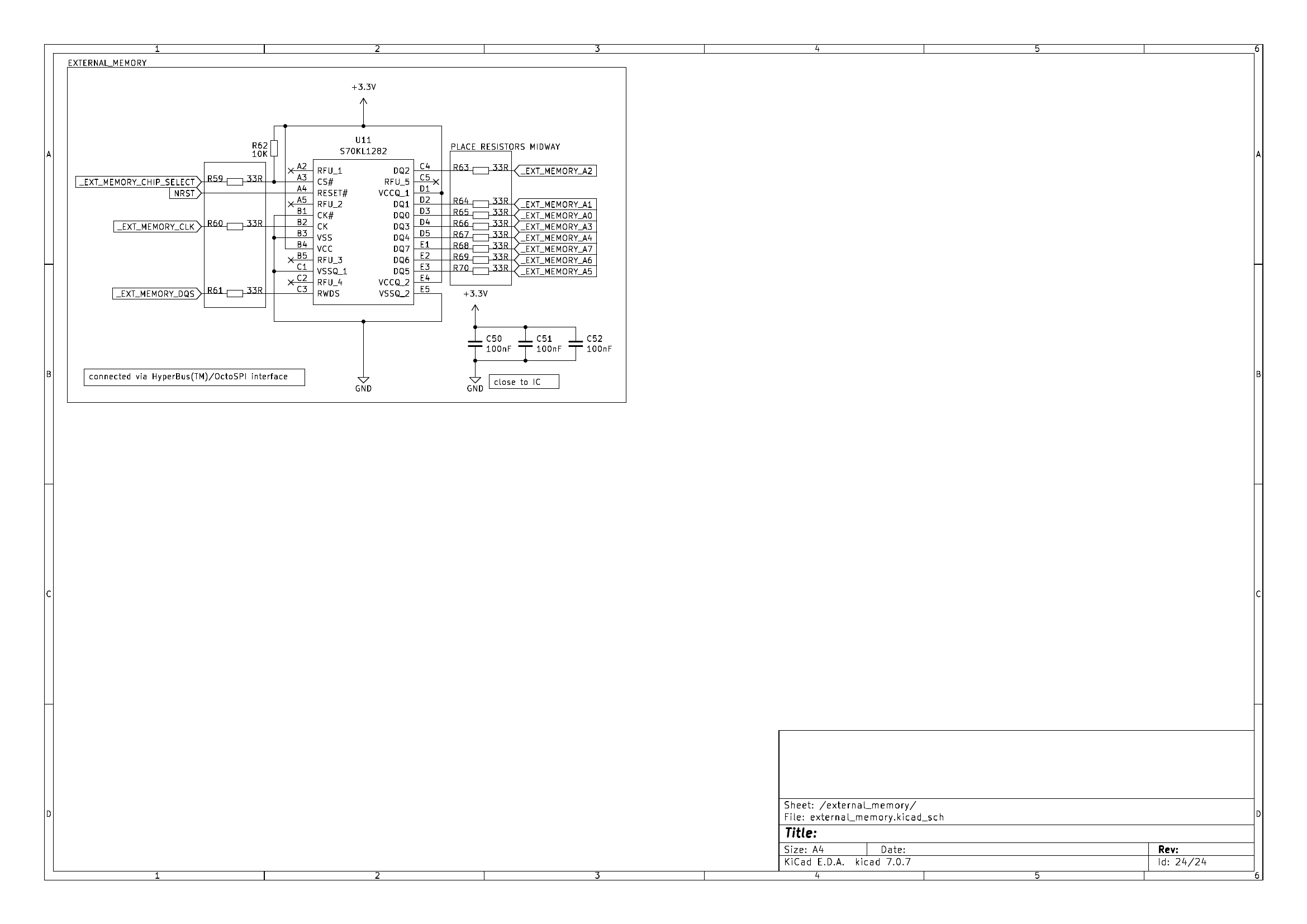
external memory is provided by S70KL1282 by Infineon ( or more specifically S70KL1282GABHV020 ), a 16MB ( or 128Mb ) DRAM with HYPERBUS™ interface
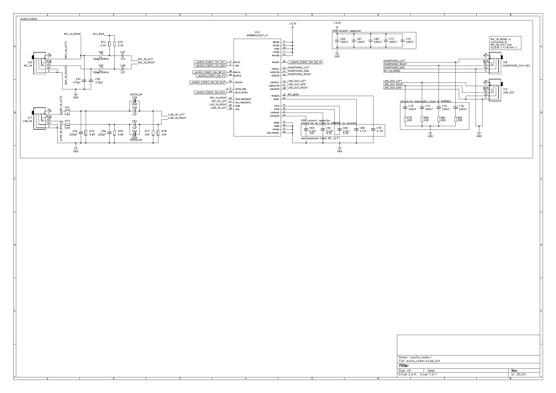
the audio codec is a WM8904 by Cirrus Logic. it features stereo headphone amplifiers in a QFN-32 package. it can be interface via a stereo line-in ( 3.5mm, TRS ), a stereo line-out ( 3.5mm, TRS ) or a 3-ring audio connector ( 3.5mm, TRRS with CTIA allocation ) for stereo headphones and mono microphone.
Power … done