PCB Build-Up + Stack-Up

TL;DR this is the KLST_PANDA stack-up:
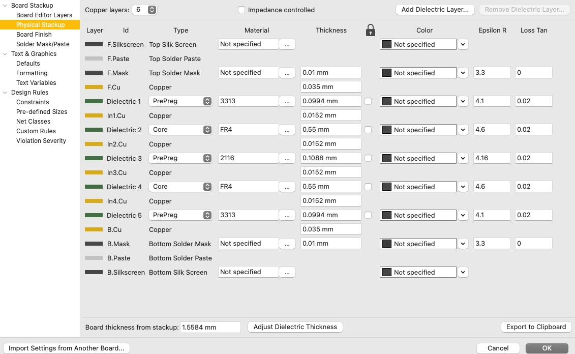
1. F.Cu   > SIG*
2. In1.Cu > GND
3. In2.Cu > SIG*
4. In3.Cu > PWR
5. In4.Cu > GND
6. B.Cu   > SIG*
long version
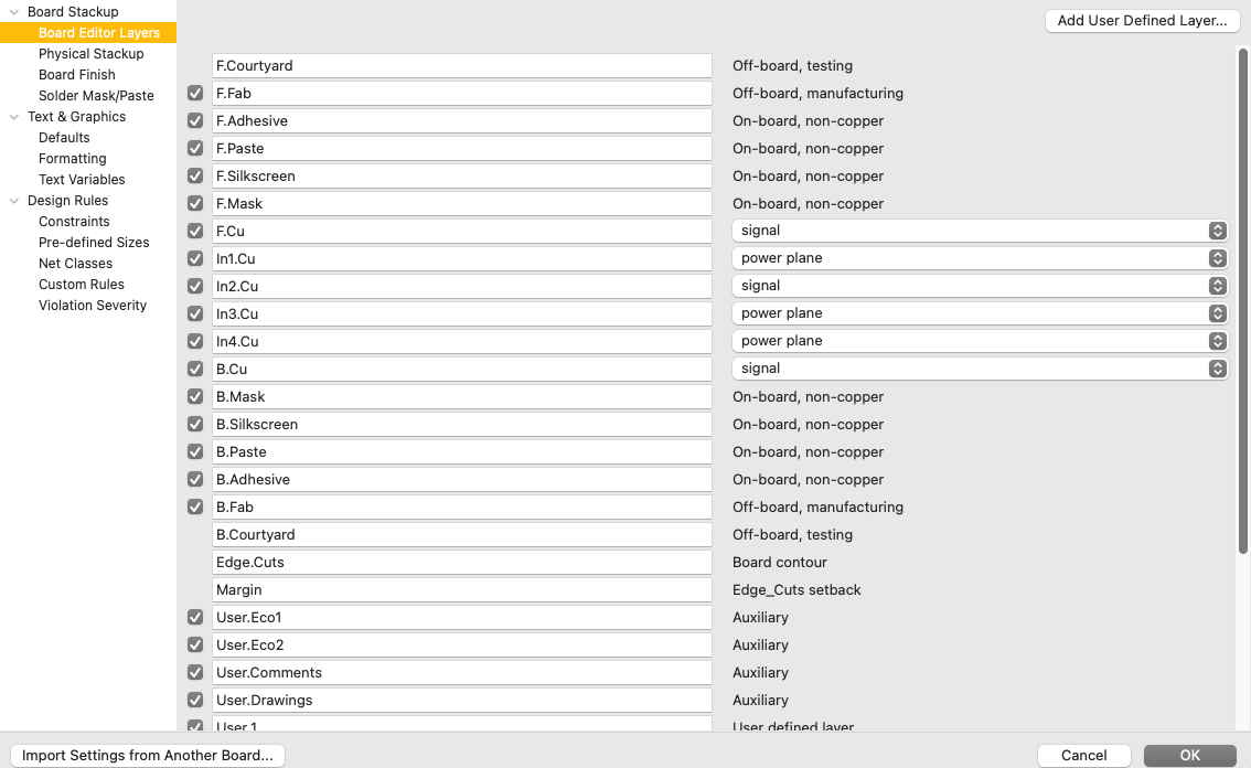
KLST_PANDA will be a 6-layer high precision PCB in black & white. according to the specification by JLCPCB ( see JLC06161H-3313 Stackup ) this will result into the following build-up:
+ ---------- +
+ C1 COPPER  +
+ D1 PREPREG +
+ C2 COPPER  +
+ ---------- +
| D2 CORE    |
+ ---------- +
+ C3 COPPER  +
+ D3 PREPREG +
+ C4 COPPER  +
+ ---------- +
| D4 CORE    |
+ ---------- +
+ C5 COPPER  +
+ D5 PREPREG +
+ C6 COPPER  +
+ ---------- +
according to Phil’s Lab #56: PCB Stack-Up and Build-Up a stack-up can look like this ( “power planes adjacent to signal planes” ):
+ ---------- +
+ C1 SIG     +
+ D1 PREPREG +
+ C2 GND     +
+ ---------- +
| D2 CORE    |
+ ---------- +
+ C3 SIG     +
+ D3 PREPREG +
+ C4 PWR     +
+ ---------- +
| D4 CORE    |
+ ---------- +
+ C5 GND     +
+ D5 PREPREG +
+ C6 SIG     +
+ ---------- +
or for short and mapped to KiCad layer names ( see TL;DR above ):
1. F.Cu   > SIG*
2. In1.Cu > GND
3. In2.Cu > SIG*
4. In3.Cu > PWR
5. In4.Cu > GND
6. B.Cu   > SIG*
and added to the KiCad project the stack-up looks like this:
and the parameters for the build-up like this:
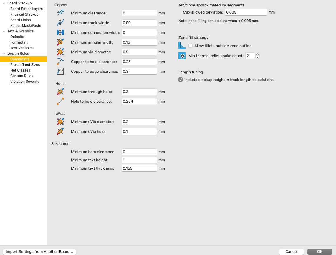
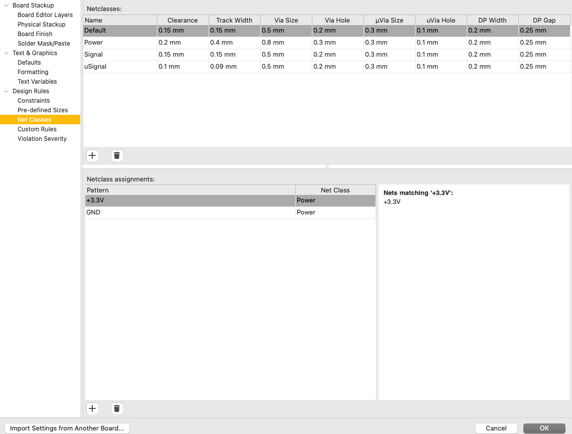
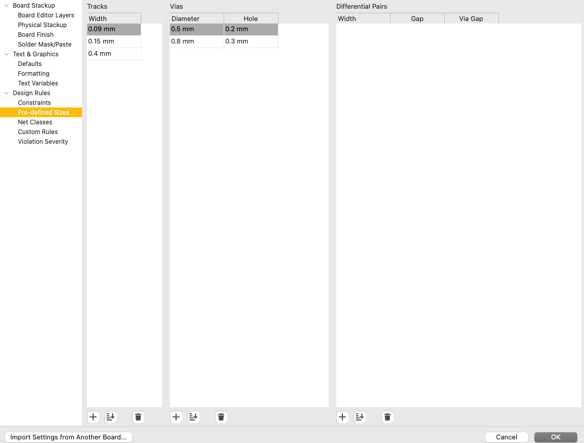
Design Rules
i have decided to apply the following PCB design rules:
- use min
0.15mmtraces ( = 0.9amp ) for signal - use min
0.15mmannular rings (0.13mmis JLCPCB min @ 1oz Cu )
| NETCLASS | CLEARENCE | TRACK WIDTH | VIA SIZE | VIA HOLE |
|---|---|---|---|---|
| SIGNAL | 0.15mm | 0.15mm | 0.5mm | 0.2mm |
| uSIGNAL | 0.10mm | 0.09mm | 0.5mm | 0.2mm |
| POWER | 0.15mm | 0.40mm | 0.8mm | 0.3mm |
| POWER DELIVERY | 0.25mm | 0.60mm | 1.0mm | 0.4mm |
see JLCPCB / PCB Manufacturing & Assembly Capabilities
and added to the KiCad project the rules looks like this: