KLST_PANDA+ADC+DAC
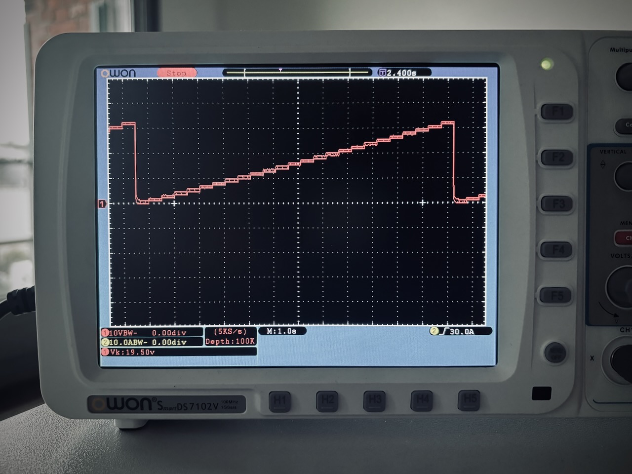 DAC stepping through the full voltage range from 0.0–3.3V
KLST_PANDA features an ADC1 and a DAC exposed via 3.5mm audio jacks. both audio connectors are configured so that TIP carries input or output signal while RINGS and SLEEVE are tied to GND.
the DAC has a voltage range from 0.0–3.3V and a resolution of 12-bit. it is also reverse voltage protected. the DAC uses the peripheral DAC1.
the ADC is clamped at a voltage range from 0.0–3.3V. the ADC is clocked at ADC at 64MHz but takes one-shot measures at speed of 2.5 cycles2. the ADC uses peripheral ADC3.